RAMINDEX and the Cortex-A76 L1I Cache
Table of Contents
An article about experimenting with the RAMINDEX feature on Arm Cortex-A76 cores.
Setting up the Stack
A few years ago while looking through some Arm documentation, I saw that some
Arm cores have a special set of EL3 system registers that present a debugging
feature called RAMINDEX which allows you to read from internal SRAMs inside
the core.
Around that time, there was also
a very cool IEEE article
published about using RAMINDEX to inspect the data caches on some Arm
machines during runtime (also see the kernel module at weirdindiankid/cacheflow).
Most parts with support for this allow you to read directly from the L1/L2 caches, and some even allow you read from different memories used for branch predictor storage.
This is generally documented in the Technical Reference Manual (TRM) for the Arm cores that support it, and as far as I'm aware, this interface is specific to cores implemented by Arm. Presumably, other organizations implementing cores based on the Arm architecture (ie. Apple, Qualcomm, NVIDIA, etc) are not required to implement and/or expose interfaces like this to programmers.
Anyhow, I think this is an extremely cool feature and I've always wanted to play around with it in some capacity, but until very recently I haven't gone out of my way to find some hardware and dedicate time to it.
This article describes the fun I had setting all this up, some tools I wrote, and then a brief [and inconclusive!] analysis about how instructions are seemingly represented in the L1I cache on the Cortex-A76.
Booting a Raspberry Pi 5
Since I'm mostly interested in Arm cores that aren't microcontrollers, I thought the Cortex-A76 cores on the Raspberry Pi 5 would be the easiest [and most inexpensive] target.
The board has a 3-pin UART/SWD port, so I ended up grabbing one of those Raspberry Pi Debug Probes with the intention of playing around with SWD on top of all this. On my way back from the local Microcenter1, it was easy to imagine what the process would look like:
-
Figure out how to run code immediately after the Cortex-A76 cores are online
-
Write some skeletal program that performs minimal configuration and then waits around in a loop [until we connect with our probe]
-
Play with debugging over SWD and the
RAMINDEXinterface
After reading up on the Raspberry Pi documentation,
I was relieved to see that the second-stage bootloader lets you specify an
"armstub" binary in the boot config. This is apparently loaded at physical
address 0x0 by the GPU, and serves as the entrypoint when the Cortex-A76
cores come out of reset. As far as I'm aware, this is typically some
build of Trusted Firmware-A.
I set up a little environment for booting over the network, and wrote a
bare-minimum armstub
(see eigenform/pirite) that leaves
all the cores idling with wfe in EL3. I figured that I'd be
doing all my experiments with the debugger, and that we'd end up halting
all of the cores when we eventually connect to the machine.
The first thing I did was try using openocd to play with SWD, which seems to
work perfectly fine. However, I was immediately confused when trying to
perform MSR/MRS, and on further inspection, it seems like there isn't too
much support for aarch64 features in the main branch.2
Writing a CMSIS-DAP Server
I usually learn a lot while hacking at things with some kind of goal in mind,
so rather than waste the opportunity, I thought I'd turn this minor
inconvenience into some kind of bespoke
CMSIS-DAP driver
that I can fit to my own purposes. I ended up using my little server and client
library (see eigenform/daphne) for
the experiments described in this article.
I learned a ton of stuff writing this, but I'll try to spare you the details. Thankfully, the Arm documentation3 on all of this (and most Arm documentation in general) is quite good, and I don't feel like I can do a better job here.
At the least, it's probably sufficient to understand that all of this works by using SWD to perform indirect accesses on the various control registers for different debugging components.
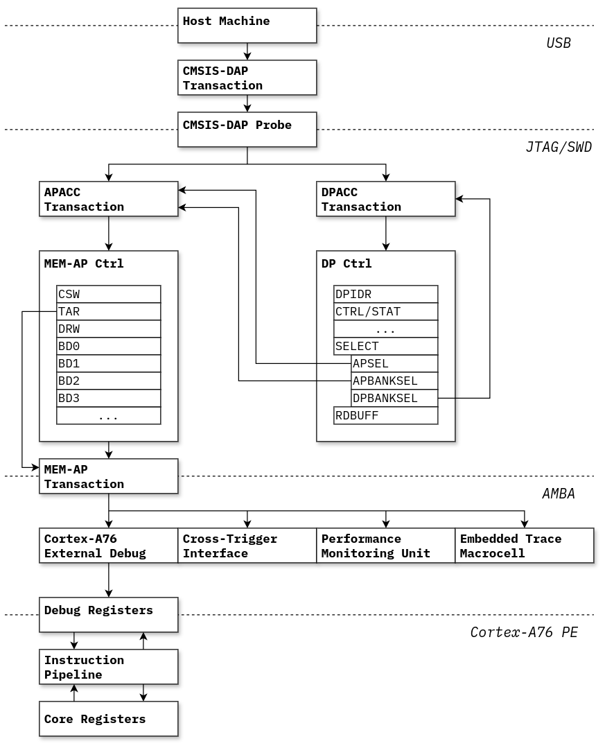
Figure 1. A block diagram showing the relationships between different protocols used during communication between my host machine and the target device.
In this case, we're mostly going to be interacting with the "external debug" interface connected to a Cortex-A76 PE. Some AArch64 system registers are shared between the PE and the debug interface, and this allows us to execute instructions and move data to and from the debugger. We also end up having to use the Cross-Trigger Interface (CTI) a little bit, but we won't need to go into any details, and we only really need this for bringing the PE in and out of the debug state.
Controlling an Armv8 PE
In the Arm architecture, there's a special "debug state" that allows a debugger to manually insert instructions into the instruction pipeline. Rather relying on the core to fetch instructions from memory, we're expected to write instructions directly into something called the Instruction Transfer Register (ITR). On top of that, there's also a Data Transfer Register (DTR), which is another special register that can be read/written from both the PE and the debugger.
Using both of these, we can control our Cortex-A76 cores and interact with the
state of the machine (ie. the general-purpose registers, system registers, and
physical memory).
As a quick example of what that looks like, let's say we wanted to write
0xdead to some general-purpose register. All we need our debugger to do is:
- Write
0xdeadto the DTR - Write
mrs x0, DTR_EL1to the ITR
This causes the core to execute mrs x0, DTR_EL1, which will set the value in
x0 to 0xdead. If we instead wanted to read data from x0, all we'd need
to do is write msr DTR_EL1, x0 to the ITR, and then use the debugger to read
value back from the DTR.
About RAMINDEX operations
With our cores halted in the debug state, we can perform a read operation
by writing to the low 32 bits in the RAMINDEX system register.
Afterwards, data is available in the IDATA{0,1,2}_EL3 system registers.
These registers are at least partially documented in the Cortex-A76 TRM4, and since I haven't heard of anyone actually using this to look at anything other than the data caches, I thought it would be fun to try reading from the L1I cache.
In this case, when performing reads, the TRM mentions that the layout of the
RAMINDEX register should look like this when reading from the L1I cache:
[31:24] RAMID = 0x01
[23:20] Reserved
[19:18] Way
[17:14] Reserved
 [13:3] Index [13:3]
  [2:0] Reserved
Looking at it for the first time, I get the impression that the index bits are only loosely documented here. Note that on the Cortex-A76, the L1I cache has the following properties:
- 64KiB total capacity
- 4-way set-associative
- 64-byte cache lines
This means that each way must contain (64KiB / 4 / 64B) == 256 sets, and
that there are probably 8 bits used to select a set.
My first guess is that the high 8 bits probably select the set, and the
remaining low 3 bits are used to select a word. In that case, our writes to
the RAMINDEX register will look like this:
[31:24] RAMID = 0x01
[23:20] Reserved
[19:18] Way
[17:14] Reserved
 [13:6] Set index?
  [5:3] Word index?
  [2:0] Reserved
The TRM also loosely describes about the format of data returned in the
IDATA registers, but we'll probably spend the rest of the article
trying to understand this in more detail:
IDATA0[63:0] - Data[63:0]

IDATA1[63:9] - Zero
IDATA1[8]    - Parity
IDATA1[7:0]  - Data[71:64]

IDATA2[63:0] - Zero
Ignoring the parity bit, it looks like these are 72-bit words. This seems to match our expectation that there are 3 bits for selecting a word within the set. Presumably there are 8 of these 72-bit words within the set, which is pretty close to 64B (about 8 64-bit words, or 16 32-bit words).
Reading the L1I Cache
As a quick sanity test, I thought I'd try adding some code to pirite that
fills the L1I cache with nop before waiting for the debugger.
That way, it should be easy to at least see some kind of output that
should correspond to known instructions.
#[unsafe(no_mangle)]
unsafe fn armstub_main() -> ! {
    // ...

    // Fill the L1I cache with nop
    core::arch::asm!(r#"
        .balign 65536
        .rept 16384
        nop
        .endr
    "#);

    // Wait around for the debugger
    loop {
        core::arch::asm!("wfe")
    }
}
At this point, we can try to read some L1I cachelines. I wrote a simple test
with the daphne library that uses RAMINDEX to exhaustively read out each
of the L1I entries. After running through 64KiB of nop, it seems like most
of the L1I cache now looks like this (omitting all the other sets for brevity):
...
set=00000010 word=000 6000113af6000113af
set=00000010 word=001 6000113af6000113af
set=00000010 word=010 6000113af6000113af
set=00000010 word=011 6000113af6000113af
set=00000010 word=100 6000113af6000113af
set=00000010 word=101 6000113af6000113af
set=00000010 word=110 6000113af6000113af
set=00000010 word=111 6000113af6000113af
...
Most importantly, it seems like each 72-bit word here is actually made up of
two 36-bit entries. In this case, it's extremely likely that we're looking at some
representation of two nop instructions (6000113af 6000113af).
On top of that, our guesses about indexing seem to be correct.
If each word in L1I data RAM is 72-bits, the 8 words in this set
correspond to 16 32-bit nop instructions here.
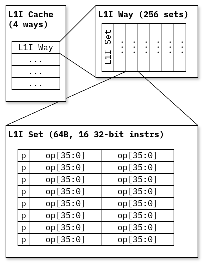
Figure #2. L1I cache (data SRAM) organization on the Cortex-A76, in the case where a cacheline is filled with 32-bit instruction encodings.
Another important thing is that the typical 32-bit encoding for nop
(0xd503201f) doesn't obviously seem to show up here!
Instead, it seems like our instructions are stored in some different
kind of format.
Without looking into it any further, it's interesting to think about what could be going on here. Is this some totally different format from the 32-bit instruction encodings, or are the bits just being rearranged in some way?
Since this is the L1I cache (and not an op cache), I think we can immediately
rule out the possibility of these being some "micro-op" representation of
instructions. These bits haven't even reached the instruction decoders yet,
and it's likely that they're mostly unchanged despite the fact that these
examples don't obviously resemble the nop encoding.
At this point, my guess is that these are either some slightly "pre-decoded" form of instructions, or that the process of fetching an L1I line simply ends up rearranging all the original bits into a more comfortable [whatever that means] internal format.
Designing an Experiment
Rather than recompiling our armstub every time, it would be really nice to
devise some process where we can use our debugger to easily insert particular
instructions into the L1I cache. This would make our attempts at understanding
the data format much easier.
As far as I'm aware, the RAMINDEX interface only permits read access to
memories, and we cannot use it to directly perform writes into the SRAM.
This means we want to find some way of causing instruction fetch and L1I fill
from our external debugger.
I originally hoped that you could do this without leaving the debug state, and it isn't too much of a stretch to imagine that we could use the ITR to do this by:
-
Executing some kind of branch with the ITR.
After this executes, the target line should [always] be in the L1I. -
Executing some prefetch instruction (ie.
prfm plil1strm) with the ITR.
After this executes, the target line should [hopefully!] be in the L1I.
However, after trying both of these, it turns out that they both cause some kind of undefined exception on the Cortex-A76 when we're using the ITR in the debug state.
Looking at the Arm ARM5, it seems like the program counter is actually undefined when the PE is in the debug state, and that we cannot expect that accesses to the program counter will behave normally. In hindsight, this should be expected since the ITR is the only way that instructions enter the pipeline in the debug state: there's simply no need for a program counter here.
I also didn't realize that there are constraints on exactly which instructions can be executed with the ITR, and that these instructions are simply not supported. As it turns out, the manual lists only a limited set of AArch64 instructions whose behavior is actually defined when using the ITR.
Controlling Instruction Fetch
Although we seemingly cannot cause the machine to fetch instructions while remaining in the debug state like this, there's nothing stopping us from simply exiting the debug state and resuming normal execution. All the debugger needs to do is send a "restart event" to the PE by poking the CTI control registers.
In order to handle switching in and out of the debug state, the DLR_EL0
system register (literally a "debug state link register") holds the value of
the program counter when the PE initially entered the debug state.
When the PE exits the debug state, normal execution resumes at the address in
DLR_EL0.
Thankfully, we can also write to DLR_EL0 using msr and the ITR.
This means we can cause instruction fetch to resume at any address we'd like.
Additionally, by inserting the hlt instruction (or any other instruction
that halts into the debug state) at the start of our
cacheline, we can guarantee that the PE will immediately return to the debug
state after the target cacheline has been fetched and brought into the L1I.
From the viewpoint of our debugger, the process of testing a single instruction encoding would look like this:
-
Write
strinstructions to the ITR which perform the following:- Write
hltat the start of the target cacheline - Write padding instructions to the entire line
- Write an instruction we want to probe at the end of the line
- Write
-
Write some instruction to the ITR that invalidates the target cacheline
(I'm just usingic iallu) -
Write
msr DLR_EL0, x0to the ITR, settingDLR_EL0to the address of the target cacheline. -
Force the PE to exit the debug state by writing to a CTI control register.
Then, wait for the PE to halt again.
Then immediately afterwards on the PE:
-
The PE starts fetching at
DLR_EL0and causes L1I fill. -
Our target cacheline is guaranteed to be in the L1I.
Thehltinstruction completes and retires.
Our tested instruction does not enter the pipeline. -
The PE re-enters the debug state.
This is also useful because, presumably, the PE will not decode and execute
all of the instructions in our target cacheline before encountering the
hlt instruction. This way, we should be able to inspect instructions that
might be liable to cause some kind of exception during or after instruction
decode.
After this, we're free to use RAMINDEX and read out the L1I bits that
correspond to our tested instruction at the end of the cacheline.
This seems to work perfectly for me, although the process is sort of slow
because we're performing lots of operations with the debugger.
Luckily in my environment, the location of the target cacheline is deterministic enough that the L1I set and way are always the same across reset. When testing different instructions, I found that it's sufficient to change only the last words in the line, and that this makes things noticeably faster.6
About AArch64 Instructions
With that sorted out, it would also be nice if we had a big list of all the valid AArch64 instruction encodings. If we can collect enough samples of instruction encodings and their associated L1I encodings, it might be easier to tell exactly what the difference is.
Thankfully, Arm publishes a machine-readable version of the ISA7 in XML, and AArch64 instructions are specified in something called the Architecture Specification Language (ASL)8.
Using a bit of Python (see alastairreid/mra_tools),
we can easily recover the ASL from these XML files, and with a little more
effort (see eigenform/aslfun) we can
walk the decoder tree and pull out 32-bit masks and matching values that are
sufficient to give us a minimal "template" for each unique instruction encoding.
Doing this with the latest release, I'm reminded that there are now apparently
lots different AArch64 instruction encodings:
$ ./parse.py
...
[*] There are 5591 encodings
[*] Stats: {
 "reserved": 1,
 "UNPREDICTABLE": 461,
 "sme": 838,
 "UNALLOCATED": 792,
 "sve": 1328,
 "dpimm": 44,
 "control": 134,
 "dpreg": 151,
 "simd": 843,
 "ldst": 999
}
Since the format of an instruction encoding changes with different operations, I figured testing with these templates would be a useful starting point. If the L1I encoding is very regular, this should make it trivial to distinguish the "decoder-relevant" bits from operands and immediate data.
Although the entire point of using the MRA was mostly to avoid manually transcribing all the encodings from the Arm ARM, I sort of ended up doing this anyway while writing a [very slow!] AArch64 decoder for use when analyzing samples. When reasoning about things, I thought it'd be useful to have some way of programatically accessing the fields defined for different groups of instruction encodings.
As an aside (and brief refresher on AArch64 encodings), note that there are seemingly ~3 levels of tables that distinguish a particular instruction, and that the top-level table looks like this:
class AArch64Table(EncodingTable):
    """ Top-level AArch64 instruction encoding """
    fields = {
        "op0": BitField(31, 31),
        "op1": BitField(28, 25),
    }
    cases = [
        EncodingCase("reserved",    op0=0, op1="0000"),
        EncodingCase("sme",         op0=1, op1="0000"),
        EncodingCase("sve",                op1="0010"),
        EncodingCase("unalloc",            op1="00x1"),
        EncodingCase(DpImmTable(),         op1="100x"),
        EncodingCase(BrnSysTable(),        op1="101x"),
        EncodingCase(DpRegTable(),         op1="x101"),
        EncodingCase(DpSimdTable(),        op1="x111"),
        EncodingCase(LdstTable(),          op1="x1x0"),
    ]
... and here's an example of what the register data-processing
instructions (DpRegTable) look like. In this case, the Logical
table is terminal and contains a group of instructions that all share
the same layout:
class DpRegTable(EncodingTable):
    ...

    class Logical(EncodingTable):
        fields = {
            "sf":    BitField(31, 31),
            "opc":   BitField(30, 29),
            "shift": BitField(23, 22),
            "N":     BitField(21, 21),
            "rm":    BitField(20, 16),
            "imm6":  BitField(15, 10),
            "rn":    BitField(9, 5),
            "rd":    BitField(4, 0),
        }
        cases = [
            EncodingCase("and",  opc=0b00, N=0),
            EncodingCase("bic",  opc=0b00, N=1),
            EncodingCase("orr",  opc=0b01, N=0),
            EncodingCase("orn",  opc=0b01, N=1),
            EncodingCase("eor",  opc=0b10, N=0),
            EncodingCase("eon",  opc=0b10, N=1),
            EncodingCase("ands", opc=0b11, N=0),
            EncodingCase("bics", opc=0b11, N=1),
        ]
    ...

    fields = {
        "op0": BitField(30, 30),
        "op1": BitField(28, 28),
        "op2": BitField(24, 21),
        "op3": BitField(15, 10),
    }
    cases = [
        EncodingCase(Dp2Src(), op0=0, op1=1, op2=0b0110),
        EncodingCase(Dp1Src(), op0=1, op1=1, op2=0b0110),
        EncodingCase(Logical(),       op1=0, op2="0xxx"),
        ...
    ]
Collecting Samples
With all of this setup out of the way, I spent some time collecting lots of samples for different instruction encodings. Frankly, I started to get bored after collecting about ~250K samples of unique valid instruction encodings. I ended up trying a couple different strategies:
- Setting or unsetting all free bits in all templates
- Randomly generating 32-bit numbers and taking the valid results
- Randomly applying masks to templates and setting random bits
- Exhaustively testing some groups of bits (ie.
0x0000_0000-0xfff0_0000) - Exhaustively flipping each bit in all templates
- Exhaustively flipping all pairs of two bits in all templates
The space of all possible 32-bit instructions is pretty big, but our templates give us very good starting points. Most of the samples were produced with the bit-flipping strategies since this seemed like easiest way of getting meaningful differences between valid encodings.
Wrap-up and Observations
After doing some analysis, I haven't come to any definite conclusion about how the encoding format works in general. In the interest of time, this article concludes with a few observations, notes about things I tried, and some visualizations.
If you're interested in trying any of this for yourself, my debugger and
analysis scripts live in eigenform/a76fun
(but beware, it's all very messy and pretty ad-hoc).
For reference, my analysis was mostly about trying to understand what properties [if any] are shared by the groups of instruction encodings defined in the specification. When considering a group, I thought it was useful to represent them as bitmasks. For example, here are all the immediate data-processing groups:
Group        L1I encoding                         Instruction encoding             N
DpImmTable   -----------------------1------------ ---100-------------------------- 25737
 AddSubImm   --0---------------0--0010-10-0------ ---100010----------------------- 5415
 Bitfield    --0---------------0----10-11-1-0---- ---100110----------------------- 3576
 Extract     --00--------------0----110100111---- -00100111-0--------------------- 245
 Logical     --0---------------0----10-00--0----- ---100100----------------------- 4300
 MovWideImm  --0---------------0----10-10-10----- ---100101----------------------- 5825
 PcRel       ------------------11-00100---------- ---10000------------------------ 6376
The intuition here is that the "constrained" bits (1 and 0) shared by all
encodings in a group are more likely to be "decoder-relevant" bits related to
distinguishing the group. On the other hand, most of the variable bits
(marked with -) are probably operands, immediate data, or used to
distinguish instructions within the group.
Invalid/Undefined Instructions
Looking at all the data, the first thing that seems obvious to me is that many of our template instructions are totally unsupported on the Cortex-A76, and this is reflected in the L1I output too. For example, the L1I encodings for SME and SVE instructions all appear to be almost exactly the same:
Group   L1I encoding                         N
Sme     --101110110000000-00-111111100001110 1161
Sve     --101110110000000-00-111111100001110 1671
Interestingly, I also noticed these are generally the same as the encoding for
udf, and this also appears to be the case for many other seemingly
invalid instruction encodings:
           L1I encoding                         Instruction encoding
'udf #0x0' 001011101100000000000111111100001110 00000000000000000000000000000000
Since we expect all invalid instruction encodings to act the same, it's not too surprising that their representation in the L1I cache is always the same. This seems like a special case where an instruction encoding is very obviously being "pre-decoded" into a totally different format.9
My scripts generally ignore these samples because they don't seem to give us
any information about the format in general (although, the fact that bits
[14:8] are all set here is kind of suspicious).
Apart from explicitly undefined and unsupported instructions, there's also the case of unallocated instruction encodings. The Arm ARM mentions (in section C1.1 "About the A64 instruction set"):
All encodings that are not fully defined are described as unallocated. An attempt to execute an unallocated instruction is
UNDEFINED, unless the behavior is otherwise defined in this Manual.
Interestingly, many [if not all?] unallocated instruction encodings do not have the exact same representation as in the "undefined" cases above. As an example, here are groups of some "unallocated" encodings in the immediate data-processing tables:
                L1I encoding                         Instruction encoding             N
DpImmTable      --0---------------0--111------------ ---1001------------------------- 2924
 Bitfield.unk   --0---------------0--1110-11-1-0---- ---100110----------------------- 1182
 Extract.unk    --001-------------00-11110100111---- 00010011100-----1--------------- 37
 Logical.unk    --0---------------0011110-00--0----- 0--1001001---------------------- 517
 MovWideImm.unk --0---------------0011110-10-10----- 0--1001011---------------------- 1188
My interpretation here is that, unlike the explicitly undefined or unsupported encodings from before, maybe unallocated encodings need to pass through the instruction decoder before being recognized as invalid.
Correlations between Bits
Looking at differences between all samples in the top-level groups, it's
not immediately obvious that the top-level op0/op1 fields correspond to
bits in the L1I encoding.
I thought it was interesting that all the data-processing groups have a few similar bits, but the loads/stores and system instructions do not. This is probably just because the formats for data-processing instructions are somewhat more regular.
            L1I Encoding                         Instruction Encoding             N
BrnSysTable ------------------------------------ ---101-------------------------- 25382
DpImmTable  -----------------------1------------ ---100-------------------------- 25737
DpRegTable  ------------------0-----101--------- ----101------------------------- 39546
DpSimdTable ------------------------11---------- ----111------------------------- 89211
LdstTable   ------------------------------------ ----1-0------------------------- 104357
If we naively plot correlations between bits across all samples, it seems obvious that there isn't a general one-to-one correspondence that applies in all cases. If bits are sequentially copied into the L1I encoding, we'd expect to see more pronounced [non-overlapping] left-to-right diagonal lines in a heatmap like this.
This probably tells us that bits in the L1I encoding are organized differently for different more-specific instruction classes, and that there's still some logic involved in actually decoding them.
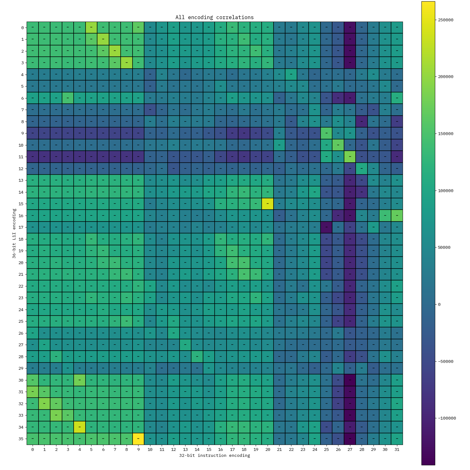
Figure 3. Correlations between bits in the instruction encoding (X-axis) and L1I encoding (Y-axis), where lighter colors indicate correlated bits and darker colors indicate anti-correlated bits.
This is easier to see if we only look at a particular top-level class of
instructions, like the immediate data-processing instructions.
In this case, it seems obvious that bits [3:0] in the instruction encoding always
map to bits [29:26] in the L1I encoding.
We can also see some places where a string of bits in the L1I encoding
potentially maps to two different places in the instruction encoding
(ie. bits [25:18] in the L1I encoding sometimes come from [12:5], and
sometimes come from [17:10]).
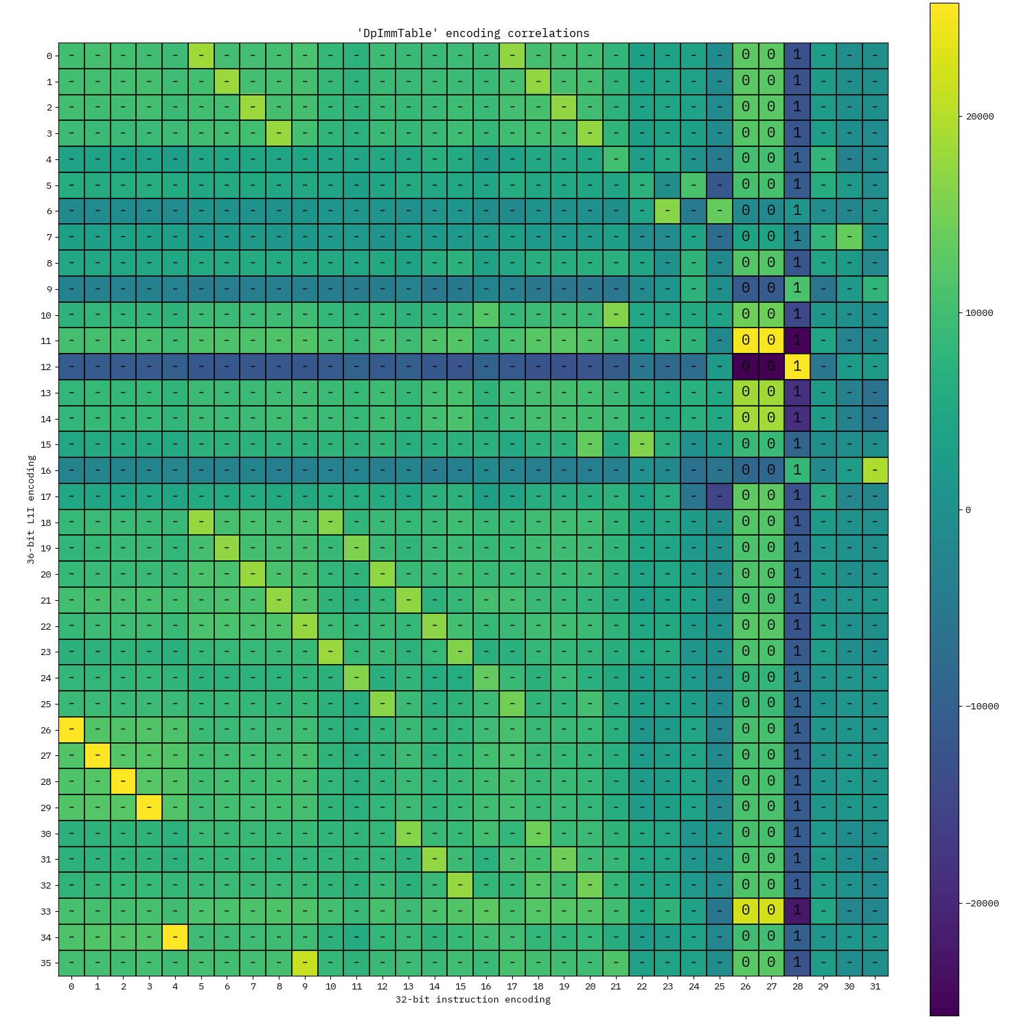
Figure 4. Correlations between bits in the immediate data-processing instruction encodings (X-axis) and L1I encoding (Y-axis), where lighter colors indicate correlated bits and darker colors indicate anti-correlated bits.
Things become somewhat more intelligible if we restrict ourselves to looking at only the terminal groups of instruction encodings. In these cases, most of the variable bits in the L1I encoding are highly correlated with a particular variable bit in the instruction encoding. Here's the heatmap for the "logical" data-processing instructions:
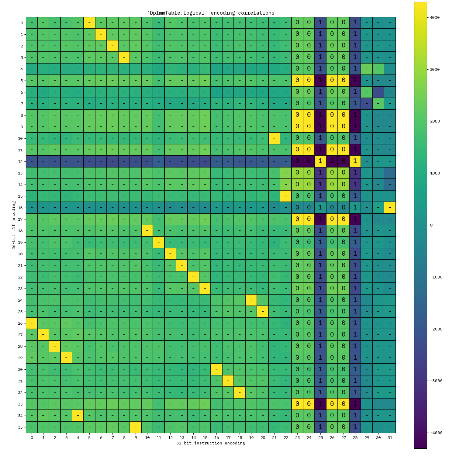
Figure 5. Correlations between bits in the "logical" immediate data-processing instruction encodings (X-axis) and L1I encoding (Y-axis), where lighter colors indicate correlated bits and darker colors indicate anti-correlated bits.
Notice that in this case, we can identify exactly where bits [22:0]
(and bit [31]) in the instruction encoding are being represented
in the L1I encoding. The rest of the highly-correlated bits (in the columns
and rows annotated with 1 and 0) are ambiguous because they're always
observed to be the same across all instruction encodings in the group.
Recovering Bitfield Diagrams
I also wrote a script that tries to infer how fields in a group of instruction encodings are represented in their L1I encodings. It definitely isn't perfect (and definitely fails to correctly identify some fields), but it works well enough that we can recover most of the easy details and visualize them as bitfield diagrams.
Within a group of instruction encodings, this script only looks at L1I bits that are perfectly-correlated to only a single bit in the instruction encoding. After finding all of the correlated bits, we're just splitting them into contiguous groups and trying to match based on the known fields defined for the group.
Again, here's an example with all the immediate data-processing groups:
Data-processing immediate (Logical)


Data-processing immediate (Bitfield)


Data-processing immediate (Extract)


Data-processing immediate (Add/Sub)


Data-processing immediate (Move wide)


Data-processing immediate (PC-relative)


Figure 6. Bitfield diagrams showing relationships between the instruction encoding and the L1I encoding. The top diagram is the 32-bit instruction encoding, and the bottom diagram is the 36-bit L1I encoding. The bitstrings below the diagrams are a mask and value representing observed constant bits within the particular group.
Other Remarks
It's not obvious to me exactly how different groups of instructions are being
distinguished from one another here, although I'm left with a feeling
that it probably involves bits [17:5].
This sort of seems to be the case for the other top-level groups too, but I
haven't arrived at a satisfying conclusion about it.
Looking at all the top-level groups like this, I also notice that that fields never seem to cross the boundary between the upper and lower 18-bits of the word. This makes me think: it isn't unreasonable to imagine that words in the L1I cache are split like this in order to accomodate both 32-bit and 16-bit instruction encodings.
The way that operand fields are being split up here might also tell you
something interesting about the underlying logic here. For instance, in
the case of these immediate data-processing groups, rather than directly
copying the register operands, the high bits (ie. rn[4] and rd[4]) are
being moved to the upper half of the word.
Following that train of thought, it's also not unreasonable to suspect that
the layout can somehow be broken up into 4-bit words.
References and Footnotes
Where I unfortunately have to report that: before leaving with my Pi5 (the 1GiB model...), I could not avoid the AoE psychic damage spreading out from the aisle filled with pricey DIMMs.
No ill-will towards the openocd maintainers here of course.
If I weren't personally allergic to C, I would have just hacked on
openocd while doing this. For reference, there's actually
an unmerged set of changes
for this that seem to apply on mainline openocd without conflict, and
they seemed to work perfectly fine for me!
I'm not actually sure if you could do this on the target without the debug state and external debugger. You'd probably have to worry about your footprint polluting the L1I cachelines that you're trying to read.
Presumably this is a special case because it's advantageous to try and identify expected invalid instructions very early in the pipeline here. I wouldn't be surprised if there's some physical design rationale for this. Maybe this gives you some slack when implementing the actual instruction decoder (ie. by trying to spread out the cost of dealing with exceptional instructions over multiple cycles).
I also wouldn't be surprised if you can use this to make instruction fetch somewhat smarter (or at least, more sanitary?). If we can easily determine where an exception is going to occur in the line, there's no sense in continuing to send younger instructions down the pipeline (since we're inevitably going to restart fetching at the exception vector anyway).